東北大学 先端スピントロニクス研究開発センター (CSIS)
スピントロニクス学術連携研究教育部門 (CSRN)
森下研究室
Morishita Laboratory
Center for Spintronics Research Network (CSRN)
Center for Science and Innovation in Spintronics (CSIS)
Tohoku University
我々は、スピントロニクス材料とダイヤモンドNV中心等の量子材料を融合した
新分野・技術に関する研究を行っています。
Our research theme is the development of new fields and technologies that integrate spintronics and quantum devices using qunatum defects, such as diamond NV centers.
新着 News
2026/05/22 中村特任研究員が第60回(2026年春季)応用物理学会講演奨励賞を受賞しました。おめでとうございます!
講演タイトル:走査型光電流顕微鏡による単一NV中心画像の空間分解能
2026/04/23 川崎君(B4)が加入しました。
2026/04/01 中村特任研究員が着任しました。
2026/03/31 石橋博士が大阪大学基礎工学研究科に助教として栄転されました。
2026/03/23 中村君が博士を取得されました。おめでとうございます!
2026/02/27 中村君(D3)がX-nics学生発表会にて、プレゼンテーション賞を受賞しました。おめでとうございます!
2026/02/ 中村君(D3)が講演が、第73回 応用物理学会 春季学術講演会の注目講演に選ばれました。講演タイトル:走査型光電流顕微鏡による単一NV中心画像の空間分解能(講演番号:18p-W9_324-8)
2026/05/22 Dr. Nakamura has received the 60th (Spring 2026) Young Scientist Presentation Award from JSAP. Congratulations!
Title of the presentation: Image Resolution of Single NV Center with Scanning Photocurrent Microscopy
2026/04/23 Mr. Mitsuki Kawasaki joined our lab as B4.
2026/04/01 Dr. Nakamura as Specially Appointed Research Fellow joined our lab.
2026/03/31 Dr. Ishibashi has been appointed as an Assistant Professor at the Graduate School of Engineering Science, Osaka University, marking a significant step forward in his career.
2026/03/23 Mr. Nakamura received his Ph.D. degree. Congratulations!
2026/02/27 Mr. Nakamura (D3) recieved the Best presentation award at X-nics Student Preseitaion.
2026/02/ Mr. Nakamura (D3) has been selected as a Highlighted Speaker at the 73rd JSAP Spring Meeting. Title of the presentation: Image Resolution of Single NV Center with Scanning Photocurrent Microscopy (Presentation No.: 18p-W9_324-8)
お知らせ Announcements
我々の研究室では、研究員、大学院生、学部4年生を募集しています。
詳しくは森下(e-mail: hiroki.morishita.d8tohoku.ac.jp)まで
Our laboratory is looking for new members, including researchers, graduate students, and undergraduate students.
For more information, please contact Prof. Morishita. (e-mail: hiroki.morishita.d8tohoku.ac.jp)
研究概要 Research
ダイヤモンドNV中心 Diamond NV center
ダイヤモンドは、炭素のみから構成されるダイヤモンド構造をもつ半導体です。リンをドーピングすることでn型ダイヤモンドが、ボロンをドーピングすることでp型ダイヤモンドが実現しています。その中で我々は、窒素と空孔がペアになった窒素―空孔(NV)中心に着目し、研究を行っています。NV中心は、室温下でも1つのNV中心のスピン状態を操作、検出することができ、長いコヒーレンス時間を有しています。そのため、室温動作可能な量子情報処理デバイスや量子センサへの応用に向けた研究が行われています。 我々は、これらの量子デバイスの集積化や高度化を目指し、ダイヤモンドNV中心のスピンの電気的検出や制御技術の確立し、スピントロニクスデバイス材料との融合した新分野を開拓しています。 Diamond is a semiconductor with a diamond structure. N-type and p-type diamond semiconductors are realized by doping phosphorus and boron, respectively. Here we use a nitrogen vacancy (NV) center in diamond. Because individual NV spins can be manipulated and detected and have a long spin coherence time, the NV center is a candidate for quantum devices, such as quantum information processing devices and quantum sensors, that operate at room temperature. We are establishing electrical detection and control techniques for diamond NV-centered spins to integrate and advance these quantum devices, and developing new fields and technologies that integrate spintronics and NV-based quantum devices.
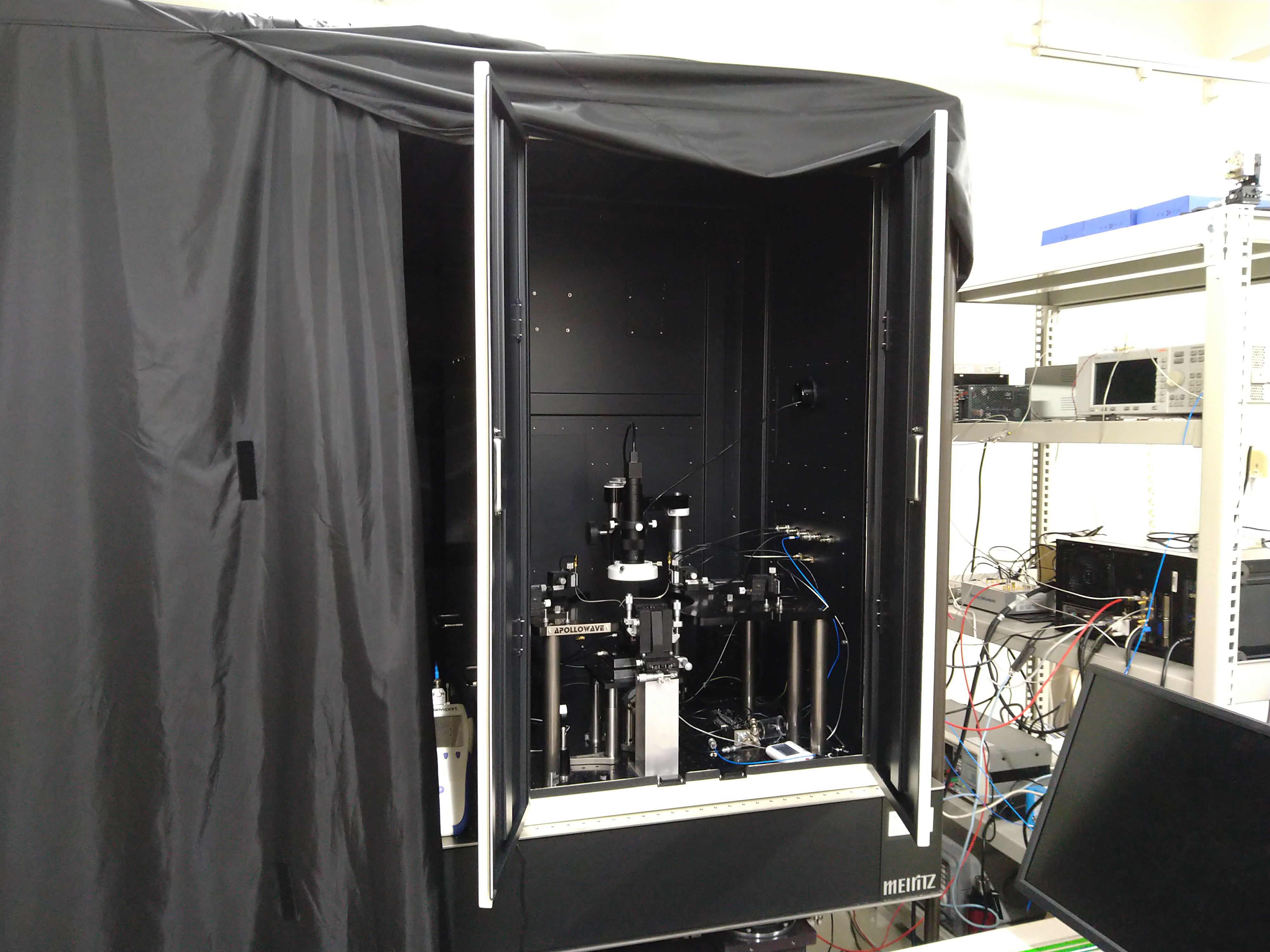
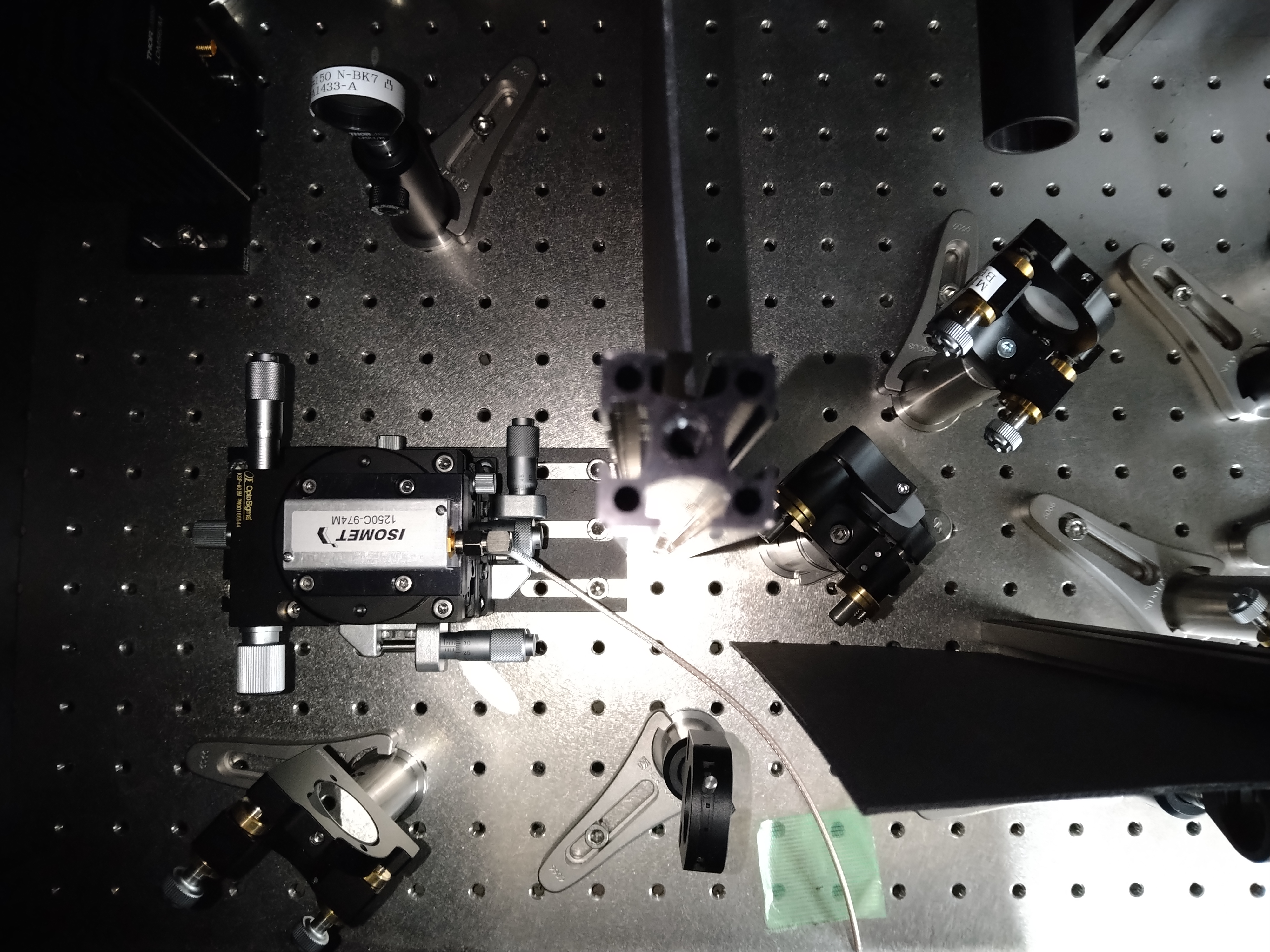
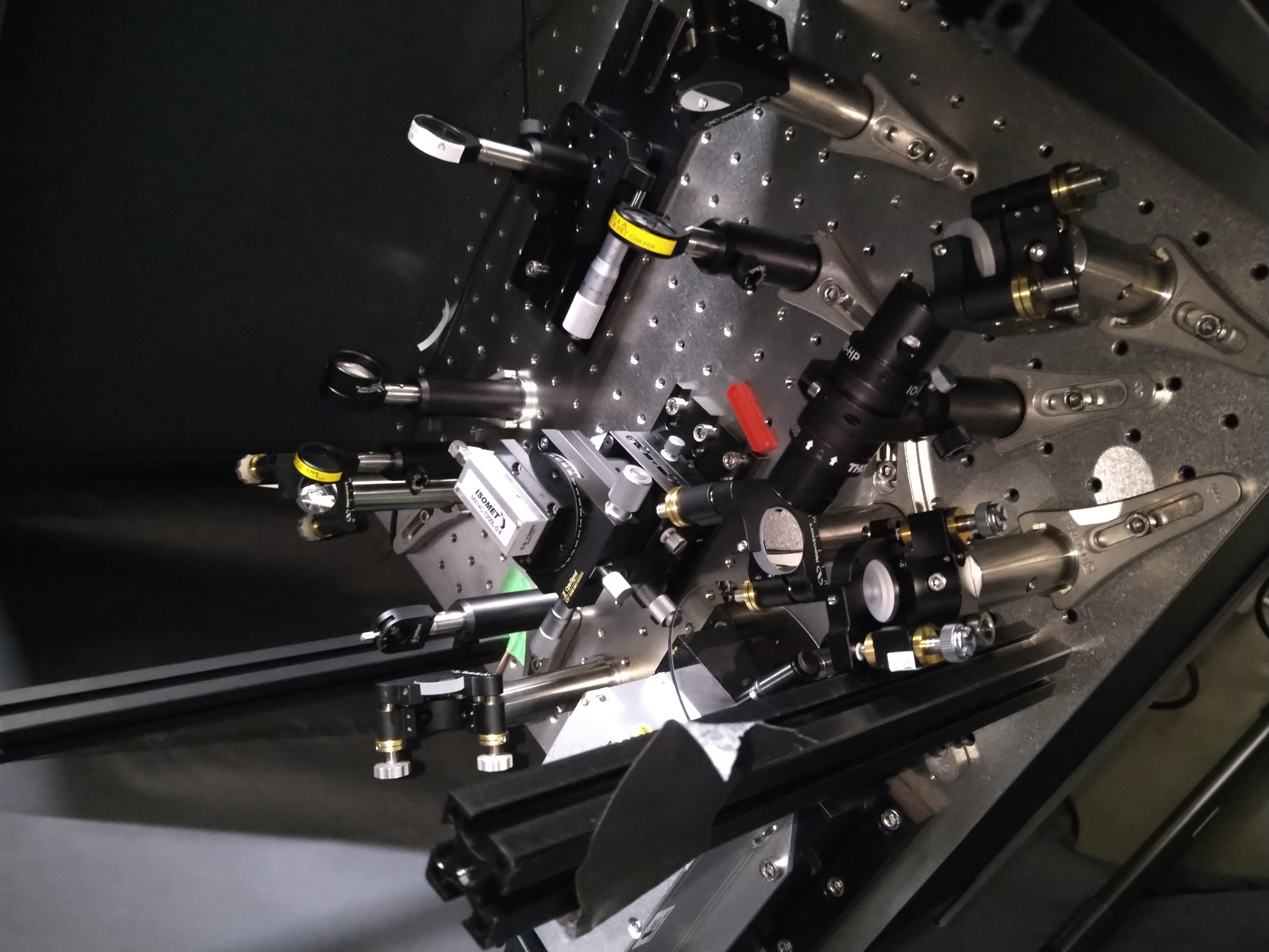
電気的磁気共鳴検出 Electrical detection of NV spins
ダイヤモンドNV中心の電気的磁気共鳴検出は、NV中心から励起される光電流量の磁気共鳴による変化を観測します。我々は、独自の電気的磁気共鳴検出装置を構築することで、NV中心の窒素核スピンコヒーレンスの電気的検出やAC磁場検出などを実証してきました。加えて、電気的的な検出技術を利用した量子デバイスの高度化に向けてその検出原理解明を行っています。
Electrical detection of NV spin measures the change in photocurrent generated from the NV center. We constructed a home-made spectrometer for the electrical detection of NV spins, and demonstrated the electrical detection of nitrogen nuclear spin coherence and AC magnetic field sensing. In addition, we understand the mechanism of the electrical detection for the development of the quantum devices using the electrical detection technique.
Physical Review Applied 19, 034061 (2023) .
NV中心の核スピンコヒーレンスの電気的検出 Electrical detection of nuclear spin coherence in NV centers
ダイヤモンド中の核スピンは環境ノイズの影響を受けにくいことから、NV中心の電子スピンと比べても長いコヒーレンス時間を有します。そのためダイヤモンド中の核スピンは、ダイヤモンド量子デバイス中で量子メモリとしての動作が期待されています。そこで、この核スピンの電気的検出を目指し、電気的電子核二重共鳴装置を開発し、室温下での核スピンコヒーレンスの電気的検出しました。本研究で観測した室温下での核スピンコヒーレンスの電気的検出は、シリコンや有機半導体を含め固体中で初めて成果になります。
本成果は、Scientific Reports, 10, 792 (2020). より報告し、Top 100 in Physics in 2020に選ばれた。
The nuclear spin in diamond has a long coherence time because it is well isolated from ambient noise. Thus, the nuclear spin is a candidate for the quantum memories in diamond quantum devices. Here, we constructed an electrically detected electron-nuclear double resonance spectrometer and detected the nuclear spin coherence at room temperature. This study shows the first demonstration of the nuclear spin coherence including solids such s silicon and organic semiconductor at room temperature.
Scientific Reports, 10, 792 (2020).(Selected as Top 100 in Physics in 2020)
電気的磁気共鳴法を利用したAC磁場検出 AC magnetic field sensing with electrical detection technique
ダイヤモンドNV中心を利用した磁気センサの研究では、NV中心のスピンの光学的な検出法を用いた実証研究が多く、電気的な手法を用いた実証研究は殆ど行われていませんでした。そこで、量子センサの小型化による集積化や高感度化を目指し、電気的検出手法を用いたAC磁場センシングを行いました。本成果は、電気的な検出手法とパルスシーケンスを用いてスピンコヒーレンスを利用したAC磁場センシングの初めての成果になります。
The electrical detection of NV spins is advantageous for the development and integration of the NV magnetometer, while most of the studies of NV magnetometers use the optical detection technique. So, we first demonstrated the AC magnetic field sensing using spin coherence with the electrical detection techniques.
Physical Review Applied 19, 034061 (2023) .
ダイヤモンドNV中心のドレスト状態 Dressed states in diamond NV center
ダイヤモンドNV中心の量子センサの高感度化に向けて、マイクロ波照射によるドレスト状態の生成やその原理解明を行っています。マイクロ波ドレスト状態は、2つのマイクロ波のNV中心に照射することで生成される状態であり、本状態を生成することで、コヒーレンス時間(T2)の長時間化などを実証し、高感度な磁場センサの提案をしています。
We study the generation and control of the dressed states of the NV center to realize highly sensitive NV quantum sensors. The dressed states are generated under the stimulated irradiation of the two microwave fields. We have first demonstrated the extension of the coherence time (T2) and propose the enhancement of the sensitivity of the NV magnetometer.
Scientific Reports, 9, 13318 (2019).
ダイヤモンドスピントロニクス Diamond spintronics
ダイヤモンドは、炭素のみで構成されているため、スピン軌道相互作用が弱いため、長いスピン拡散長がをもつことが期待されています。我々は、NiFe/p-type diamond構造を用いてNiFeの強磁性共鳴下での起電力を初めて観測し、ダイヤモンド半導体スピントロニクスデバイスの実現に向けて、ダイヤモンドへのスピン注入研究を行っています。
We study spin injection into the diamond to realize diamond semiconductor spintronic devices. They are expected to have a long spin diffusion length due to their weak spin-orbit interaction. We have first observed electromotive forces in NiFe/p-type diamond structure under the ferromagnetic resonance of NiFe.
Solid State Communications, 243, 44 (2016).
 WPI AIMR
 WPI AIMR
メンバー Members
外線は、022-217-を内線の前につけてください。
E-mailは、tohoku.ac.jpをつけて下さい。
居室は、片平キャンパス 材料科学高等研究所 AIMR別館内です。
Phone: Please dial +81-(0)22-217 before the extension.
E-mail: Please add tohoku.ac.jp.
Our rooms are located in the AIMR Annex, Advanced Institute for Materials Research, Katahira Campus.
Alumni Alumni
Staff members:
石橋一晃 2025/10 - 2026/03 大阪大学 助教
Student members:
三沢辰己 2023/04 - 2026/03 就職
研究成果 Research Results
論文リスト Publications 、 解説論文 Reviews 、 受賞 Awards 、 招待講演 Invited Talks
論文リスト Publications
* = corresponding author
† = first equlally
“Scanning photocurrent imaging resolution of single NV center in diamond,”
Shunki Nakamura, Naoya Morioka, Norikazu Mizuochi, Shigemi Mizukami, and Hiroki Morishita*
Applied Physics Letters 127, 224003 (2025) .
doi: 10.1063/5.0286279
“Compact and portable pulsed measurement module using diamond NV centers,”
Hiroshige Deguchi*, Tsukasa Hayashi, Hiroya Saito, Yoshiki Nishibayashi, Minori Teramoto, Masanori Fujiwara, Hiroki Morishita, Norikazu Mizuochi and Natsuo Tatsumi*
Japanese Journal of Applied Physics 64, 070903 (2025) .
doi: 10.35848/1347-4065/ade924
“Compact and portable diamond NV sensor module,”
Hiroshige Deguchi*, Tsukasa Hayashi, Hiroya Saito, Yoshiki Nishibayashi, Minori Teramoto, Masanori Fujiwara, Hiroki Morishita, Norikazu Mizuochi, and Natsuo Tatsumi*
Applied Physics Express 16, 062004 (2023) .
doi: 10.35848/1882-0786/acd836
“Spin-dependent dynamics of photocarrier generation in electrically detected nitrogen-vacancy-based quantum sensing,”
Hiroki Morishita*, Naoya Morioka, Tetsuri Nishikawa, Hajime Yao, Shinobu Onoda, Hiroshi Abe, Takeshi Ohshima, and Norikazu Mizuochi*
Physical Review Applied 19, 034061 (2023) .
doi: 10.1103/PhysRevApplied.19.034061
“Electroluminescence of negatively charged single NV centers in diamond,”
M. Haruyama*, H. Kato, M. Ogura, Y. Kato, D. Takeuchi, S. Yamasaki, T. Iwasaki, H. Morishita, M. Fujiwara, N. Mizuochi, and T. Makino
Applied Physics Letters 122, 072101 (2023) .
doi: 10.1063/5.0138050
“Broadband microwave antenna for uniform manipulation of millimeter-scale volumes of diamond quantum sensors,”
Y. Takemura, K. Hayashi, Y. Yoshii, M. Saito, S. Onoda, H. Abe, T. Ohshima, T. Taniguchi, M. Fujiwara, H. Morishita, I. Ohki, and N. Mizuochi*,
Journal of Applied Physics 132, 224501 (2022) .
doi: 10.1063/5.0128406
“Electrical detection of nuclear spin via silicon vacancy in silicon carbide at room temperature,”
T. Nishikawa, N. Morioka*, H. Abe, H. Morishita, T. Ohshima, N. Mizuochi*,
Applied Physics Letters 121, 184005 (2022) .
doi: 10.1063/5.0115928
“The Anomalous Formation of Irradiation Induced Nitrogen-Vacancy Centers in 5-Nanometer-Sized Detonation Nanodiamonds,”
F. T.-K. So, A. I. Shames, D. Terada, T. Genjo, H. Morishita, I. Ohki, T. Ohshima, S. Onoda, H. Takahsima, S. Takeuchi, N. Mizuochi, R. Igarashi, M. Shirakawa*, T. F. Segawa*,
The Journal of Physical Chemistry C, 126, 5206-5217 (2022) .
doi: 10.1021/acs.jpcc.1c10466
arXiv: 2112.06909
“Room Temperature Electrically Detected Nuclear Spin Coherence of NV Centres in Diamond, ”
H. Morishita*, S. Kobayashi, M. Fujiwara, H. Kato, T. Makino, S. Yamasaki, N. Mizuochi*,
Scientific Reports, 10, 792 (2020).
doi: 10.1038/s41598-020-57569-8.
arXiv: 1803.01161.
One of the top 100 downloaded physics papers for Scientific Reports in 2020.
“Electrical Control for Extending the Ramsey Spin Coherence Time of Ion-Implanted Nitrogen-Vacancy Centers in Diamond, ”
S. Kobayashi, Y. Matsuzaki, H. Morishita, S. Miwa, Y. Suzuki, M. Fujiwara, N. Mizuochi*,
Physical Review Applied, 14, 044033 (2020)..
doi: 10.1103/PhysRevApplied.14.044033.
arXiv: 2009.01990.
“Experimental and Theoretical Analysis of Noise Strength and Environmental Correlation Time for Ensembles of Nitrogen-Vacancy Centers in Diamond,”
K. Hayashi*, Y. Matsuzaki, T. Ashida, S. Onoda, H. Abe, T. Ohshima, M. Hatano, T. Taniguchi, H. Morishita, M. Fujiwara, N. Mizuochi*,
Journal of the Physical Society of Japan, 89, 054708 (2020).
doi: 10.7566/JPSJ.89.054708.
arXiv: 1907.09095.
“ Ultra-long coherence times amongst room-temperature solid-state spins, ”
E. D. Herbschleb*, H. Kato, Y. Maruyama, T. Danjo, T. Makino, S. Yamasaki, I. Ohki, K. Hayashi, H. Morishita, M. Fujiwara, N. Mizuochi*,
Nature Communications, 10, 3766 (2019).
doi: 10.1038/s41467-019-11776-8.
“ Extension of the Coherence Time by Generating MW Dressed States in a Single NV Centre in Diamond, ”
H. Morishita*,†, T. Tashima*,†, D. Mima, H. Kato, T. Makino, S. Yamasaki, M. Fujiwara, N. Mizuochi*,
Scientific Reports, 9, 13318 (2019).
doi: 10.1038/s41598-019-49683-z.
arXiv: 1707.04702
“ Experimental demonstration of two-photon magnetic resonances in a single-spin-system of a solid, ”
T. Tashima*,†, H. Morishita*,†, N. Mizuochi*,
Physical Review A, 100, 023801 (2019).
doi: 10.1103/PhysRevA.100.023801.
arXiv: 1712.04615.
“ Optimization of Temperature Sensitivity Using the Optically Detected Magnetic-Resonance Spectrum of a Nitrogen-Vacancy Center Ensemble, ”
K. Hayashi*, Y. Matsuzaki, T. Taniguchi, T. Shimo-Oka, I. Nakamura, S. Onoda, T. Ohshima, H. Morishita, M. Fujiwara, S. Saito, N. Mizuochi*,
Physical Review Applied, 10, 034009 (2018).
doi: 10.1103/PhysRevApplied.10.034009.
“ Engineering of Fermi level by nin diamond junction for control of charge states of NV centers, ”
T. Murai, T. Makino, H. Kato, M. Shimizu, D. E. Herbschleb, Y. Doi, H. Morishita, M. Fujiwara, M. Hatano, S. Yamasaki, N. Mizuochi*,
Applied Physics Letters, 112, 111903 (2018).
doi: 10.1063/1.5010956.
News in AIP Publishing
“ Electron paramagnetic resonance study of MgO thin-film grown on silicon, ”
K. Hayashi, Y. Matsumura, S. Kobayashi, H. Morishita, H. Koike, S. Miwa, N. Mizuochi, Y. Suzuki,
Journal of Applied Physics, 121, 213901 (2017).
doi: 10.1063/1.4983752
“ Ferromagnetic-resonance induced electromotive forces in Ni81Fe19 | p-type diamond, ”
N. Fukui, H. Morishita*, S. Kobayashi, S. Miwa, N. Mizuochi*, Y. Suzuki,
Solid State Communications, 243, 44 (2016).
doi: 10.1016/j.ssc.2016.06.001
“ Optically detected magnetic resonance of high-density ensemble of NV- centers in diamond, ”
Y. Matsuzaki*, H. Morishita, T. Tashima, K. Kakuyanagi, K. Semba, W. J. Munro, H. Yamaguchi, N. Mizuochi, S. Saito,
Journal of Physics: Condensed Matter, 28, 275302 (2016).
doi: 10.1088/0953-8984/28/27/275302.
arXiv: 1508.04501
“ Pure negatively charged state of the NV center in n-type diamond, ”
Y. Doi, T. Fukui, H. Kato, T. Makino, S. Yamasaki, T. Tashima, H. Morishita, S. Miwa, F. Jelezko, Y. Suzuki, N. Mizuochi*,
Physical Review B, 93, 081203(R) (2016).
doi: 10.1103/PhysRevB.93.081203.
“ Tunnel anisotropic magnetoresistance in CoFeB vertical bar MgO vertical bar Ta junctions, ”
S. Hatanaka, S. Miwa*, K. Matsuda, K. Nawaoka, K. Tanaka, H. Morishita, N. Mizuochi, T. Shinjo, Y. Suzuki,
Applied Physics Letters, 107, 082407 (2015).
doi: 10.1063/1.4929682.
“ Pulsed low-field electrically detected magnetic resonance, ”
L. Dreher*, F. Hoehne, H. Morishita, H. Huebl, M. Stutzmann, K. M. Itoh, M. S. Brandt,
Physical Review B, 91, 075314 (2015).
doi: 10.1103/PhysRevB.91.075314.
“ Perfect selective alignment of nitrogen-vacancy centers in diamond, ”
T. Fukui, Y. Doi, T. Miyazaki, Y. Miyamoto, H. Kato, T. Matsumoto, T. Makino, S. Yamasaki, R. Morimoto, N. Tokuda, M. Hatano, Y. Sakagawa, H. Morishita, T. Tashima, S. Miwa, Y. Suzuki, N. Mizuochi*,
Applied Physics Express, 7, 055201 (2014).
doi: 10.7567/APEX.7.055201.
Selected in SPOTLIGHTS
“ Mechanisms of spin-dependent dark conductivity in films of a soluble fullerene derivative under bipolar injection, ”
H. Morishita, W. J. Baker, D. P. Waters, R. Baarda, J. M. Lupton*, C. Boehme*,
Physical Review B 89, 125311 (2014).
doi:10.1103/PhysRevB.89.125311.
“ Deterministic Electrical Charge-State Initialization of Single Nitrogen-Vacancy Center in Diamond, ”
Y. Doi, T. Makino, H. Kato, D. Takeuchi, M. Ogura, H. Okushi, H. Morishita, T. Tashima, S. Miwa, S. Yamasaki, J. Wrachtrup, Y. Suzuki, N. Mizuochi*,
Physical Review X 4, 011057 (2014).
doi: 10.1103/PhysRevX.4.011057.
“ Robust absolute magnetometry with organic thin-film devices, ”
W. J. Baker, K. Ambal, D. P. Waters, R. Baarda, H. Morishita, K. van Schooten, D. R. McCamey, J. M. Lupton, C. Boehme*
Nature Communications 3, 898 (2012).
doi:10.1038/ncomms1895
Featured in a News and Views by Joseph Shinar in Nature Materials.
Featured in a News and Views by Stefano Sanvito and V. Alek Dediu in Nature Nanotechnology.
“ Electrical detection of cross relaxation between electron spins of phosphorus and oxygen-vacancy centers in silicon, ”
W. Akhtar, H. Morishita, K. Sawano, Y. Shiraki, L. S. Vlasenko, K. M. Itoh*,
Physcial Review B 84, 045204 (2011).
doi:10.1103/PhysRevB.84.045204
“ Linewidth of Low-Field Electrically Detected Magnetic Resonance of Phosphorus in Isotopically Controlled Silicon, ”
H. Morishita, E. Abe, W. Akhtar, L. S. Vlasenko, A. Fujimoto, K. Sawano, Y. Shiraki, L. Dreher, H. Riemann, N. V. Abrosimov, P. Becker, H.-J. Pohl, M. L. W. Thewalt, M. S. Brandt, K. M. Itoh*
Applied Physics Express 4, 021302 (2011).
doi: 10.1143/APEX.4.021302
Selected for the Journal's Top 20 Most Downloaded Articles on January 2011.
“ Electrical detection and magnetic-field control of spin states in phosphorus-doped silicon, ”
H. Morishita, L. S. Vlasenko, H. Tanaka, K. Semba, K. Sawano, Y. Shiraki, M. Eto, K. M. Itoh*,
Physcial Review B 80, 205206 (2009)
doi: 10.1103/PhysRevB.80.205206
Selected for the December 2009 issue (Vol. 9, Issue 12 ) of Vir. J. Quantum Inf.
“ Electrically detected magnetic resonance of phosphorous due to spin dependent recombination with triplet centers in γ-irradiated silicon, ”
W. Akhtar, H. Morishita, L. S. Vlasenko, D. S. Poloskin, K. M. Itoh*
Physica B 404, 4583-4585 (2009).
doi: 10.1016/j.physb.2009.08.116
解説論文 Reviews
“コンパクトなポータブル量子センサの開発,”
出口 洋成,林 司,済藤 紘矢,西林 良樹,寺本 三記,藤原 正規,森下 弘樹,水落 憲和,辰巳 夏生,
ニューダイヤモンド, vol.42, pp. 26-27 (2026).
“Compact and Portable Quantum Sensor Using Diamond NV Center,”
Hiroshige Deguchi, Tsukasa Hayashi, Hiroya Saito, Yoshiki Nishibayashi, Minori Teramoto, Masanori Fujiwara, Hiroki Morishita, Norikazu Mizuochi and Natsuo Tatsumi,
New Diamond, vol.42, pp. 26-27 (2026).
“ ダイヤモンド中のNV-センタの電気的励起発光, ”
春山盛善,加藤宙光,小倉政彦,加藤有香子,竹内大輔,山崎聡,岩崎孝之,森下弘樹,藤原正規,水落憲和,牧野俊晴,
ニューダイヤモンド, vol.39, pp. 19-23 (2023).
“ lectroluminescence of Negatively Charged Single NV Centers in Diamond , ”
Moriyoshi Haruyama, Hiromitsu Kato, Masahiko Ogura, Yukako Kato, Daisuke Takeuchi, Satoshi Yamasaki, Takayuki Iwasaki, Hiroki Morishita, Masanori Fujiwara, Norikazu Mizuochi and Toshiharu Makino,
New Diamond, vol.39, pp. 19-23 (2023).
“ ダイヤモンド NV 中心の電子・核スピンの電気的検出, ”
森下 弘樹,
応用物理, vol.92, pp. 425-429 (2023).
“ Electrical detection of electron and nuclear spins of NV centers in diamond, ”
Hiroki Morishita,
Oyo Buturi, vol.92, pp. 425-429 (2023).
“ Long coherence times and high magnetic sensitivity with nitrogen-vacancy centres in phosphorus-doped diamond, ”
E. D. Herbschleb, H. Kato, Y. Maruyama, T. Danjo, T. Makino, S. Yamasaki, I. Ohki, K. Hayashi, H. Morishita, M. Fujiwara, N. Mizuochi,
ニューダイヤモンドフォーラム会誌, vol.36, pp. 10-16 (2020).
“ Long coherence times and high magnetic sensitivity with nitrogen-vacancy centres in phosphorus-doped diamond, ”
E. D. Herbschleb, H. Kato, Y. Maruyama, T. Danjo, T. Makino, S. Yamasaki, I. Ohki, K. Hayashi, H. Morishita, M. Fujiwara, N. Mizuochi,
New Diamond, vol.36, pp. 10-16 (2020).
“ NV中心の窒素核スピンコヒーレンスの制御と電気的検出, ”
森下弘樹,小林悟士,藤原正規,加藤宙光,牧野俊晴,山崎聡,水落憲和,
ニューダイヤモンドフォーラム会誌, vol.34, pp. 14-18 (2018).
“ Electrical Detection and Control of Nitrogen Nuclear Spins Coherence in NV Centers, ”
Hiroki Morishita, Satoshi Kobayashi, Masanori Fujiwara, Hiromitsu Kato, Toshiharu Makino, Satoshi Yamasaki, Norikazu Mizuochi,
New Diamond, vol.34, pp. 14-18 (2018).
“ ダイヤモンドNV中心における電界によるスピンコヒーレンス時間の長時間化, ”
小林悟士,森下弘樹,松崎雄一郎,三輪真嗣,鈴木義茂,水落憲和,
ニューダイヤモンドフォーラム会誌, vol.32, pp. 11-15 (2016).
“ Enhancement of the spin coherence time in NV center under electric field, ”
Satoshi Kobayashi, Hiroki Morishita, Yuichiro Matsuzaki, Shinji Miwa, YOshishige Suzuki, Norikazu Mizuochi,
New Diamond, vol.32, pp. 11-15 (2016).
受賞 Awards
2024年 2月 IOP Outstanding Reviewer Awards 2023, Applied Physics Express 2023 February, IOP Outstanding Reviewer Awards 2023, Applied Physics Express
2023年 3月 IOP Outstanding Reviewer Awards 2022, Japanese Journal of Applied Physics 2023 March, IOP Outstanding Reviewer Awards 2022, Japanese Journal of Applied Physics
2019年 2月 Poster Award, The First International Forum on Quantum Sensing 2019 February, Poster Award, The First International Forum on Quantum Sensing
2018年 1 月 優秀講演賞 第31 回ダイヤモンドシンポジウム 2018 January, 31st Diamond Symposium Best Oral Session Award
2016 年 9 月 第38回(2016年度)応用物理学会論文賞 公益社団法人 応用物理学会 2016 September, 38th JSAP Outstanding Paper Award Recipients 2016
2011 年 3 月 Excellent Achievement Award 慶應グローバルCOE 2011 March Excellent Achievement Award, Keio Grobal COE
2010 年 8 月 Student Award, The 6th International Conference on the Physics and Applications of spin Related Phenomena in Semiconductors 2010 Augast, Student Award, The 6th International Conference on the Physics and Applications of spin Related Phenomena in Semiconductors
2008 年 3 月 主任賞 (最優秀修士論文賞) 私立慶應義塾大学大学院基礎理工学専攻応用物理専修 2008 March, The Best Senior Research Award, Center for Applied Physics and Physico-Informatics, Keio University.
招待講演 Invited Talks
国際会議 International Conference
Hiroki Morishita, “Electrical Detection and Control of Individual NV Electron Spin,”
The 3rd International Workshop of Spin/Quantum Materials and Devices & 6th Workshop on Quantum and Classical Cryogenic Devices, Circuits, and Systems, Nov. 5 - Nov. 6, 2024, Sendai, Japan.
Hiroki Morishita, “Electrically Detected Photocarrier Dynamics of NV Quantum Sensor,”
The 11th Asia Pacific Workshop on Widegap Semiconductors, Oct. 13 - Oct. 17, 2024, Busan, Korea.
Hiroki Morishita, “NV Quantum Sensing with Electrical Detection Technique,”
The 5th International Symposium on Advanced Magnetic Materials and Applications, Aug. 4 - Aug. 7, 2024, Quang Binh, Vietnam.
Hiroki Morishita, “Electrically Detected NV Quantum Sensors,”
The 7th QST International Symposium , Jul. 24 - Jul. 25, 2024, Takasaki, Japan.
Hiroki Morishita, “Electrical detection of NV spins in diamond,”
1st Workshop of the Chicago-Tohoku Quantum Alliance , Oct. 5 - Oct. 6, 2023, Sendai, Japan.
Hiroki Morishita, “Electrical Detection and Control of NV Spin,”
EU-Japan Workshop on Spintronics and Quantum Transformation (SPIN-QX 2023) , Aug. 7 - Aug. 10, 2023, Jülich, Germany.
Hiroki Morishita, “Spin-dependent dynamics of photocarrier generation in electrically detected nitrogen-vacancy-based quantum sensing,”
International Workshop of Spin/Quantum Materials and Devices, Feb. 23 - Feb. 24, 2023, Sendai, Japan.
Hiroki Morishita, “Electrically detected magnetic resonance study of NV centers in diamond,”
the 13th
New Diamond and Nano Carbons Conference, May 12 – May 17, 2019, Haulien, Taiwan.
H. Morishita and N. Mizuochi, “Diamond magnetometry based on an electrically detected magnetic resonance,”
International Symposium on Pure & Applied Chemistry 2016, Aug. 15 - Aug. 19, 2016, Kuching, Sarawak, Malaysia.
H. Morishita and K. M. Itoh, “Quantum manipulation of electron and nuclear spins in dopants in silicon,”
XIII International Conference on Quantum Optics and Quantum Information, May 28 - Jun. 1, 2010, Kyiv, Ukraine.
国内会議 Domestic Conference
森下弘樹, “電気的スピン検出を用いた ダイヤモンド量子デバイス,”
次世代量子科学・物性工学討論会, 慶応義塾大学, 横浜市,2024.
森下弘樹, “ダイヤモンドNV中心の電気的制御と検出,”
令和5年 東北大学電気通信研究所 共同プロジェクト研究会「固体中のスピン・軌道ダイナミクスとその制御」, 東北大学電気通信研究所 ナノスピン実験施設, 仙台市,2023.
森下弘樹, “ダイヤモンド NV中心の電気的検出とその応用,”
第1回 東北大学CSRNセミナー, 東北大学材料科学高等研究所(WPI-AIMR), 仙台市,2022.
森下弘樹, “電気的磁気共鳴法を用いたダイヤモンドNV 中心の量子デバイス応用,”
量子情報研究会, オンライン,2020.
森下 弘樹, “ダイヤモンドNV 中心とその応用,” 京都大学大学院工学研究科分子工専攻コロキュウム,京都大学桂キャンパス,京都市,2018.
森下 弘樹, “ダイヤモンドNV中心の電気的磁気共鳴検出,” 京都大学化学研究所第111 回研究発表会,京都大学宇治キャンパス,宇治市 2017.
森下 弘樹, “NV 中心の電気的検出磁気共鳴,” 第4 回TIA かけはしワークショップ「ダイヤモンドNV中心の量子デバイス応用」,東京大学本郷キャンパス,東京,2017.
森下 弘樹 水落 憲和, “ダイヤモンド中のスピン依存性電気特性,” 第77 回応用物理学会秋季学術講演会,朱鷺メッセ,新潟,2016.
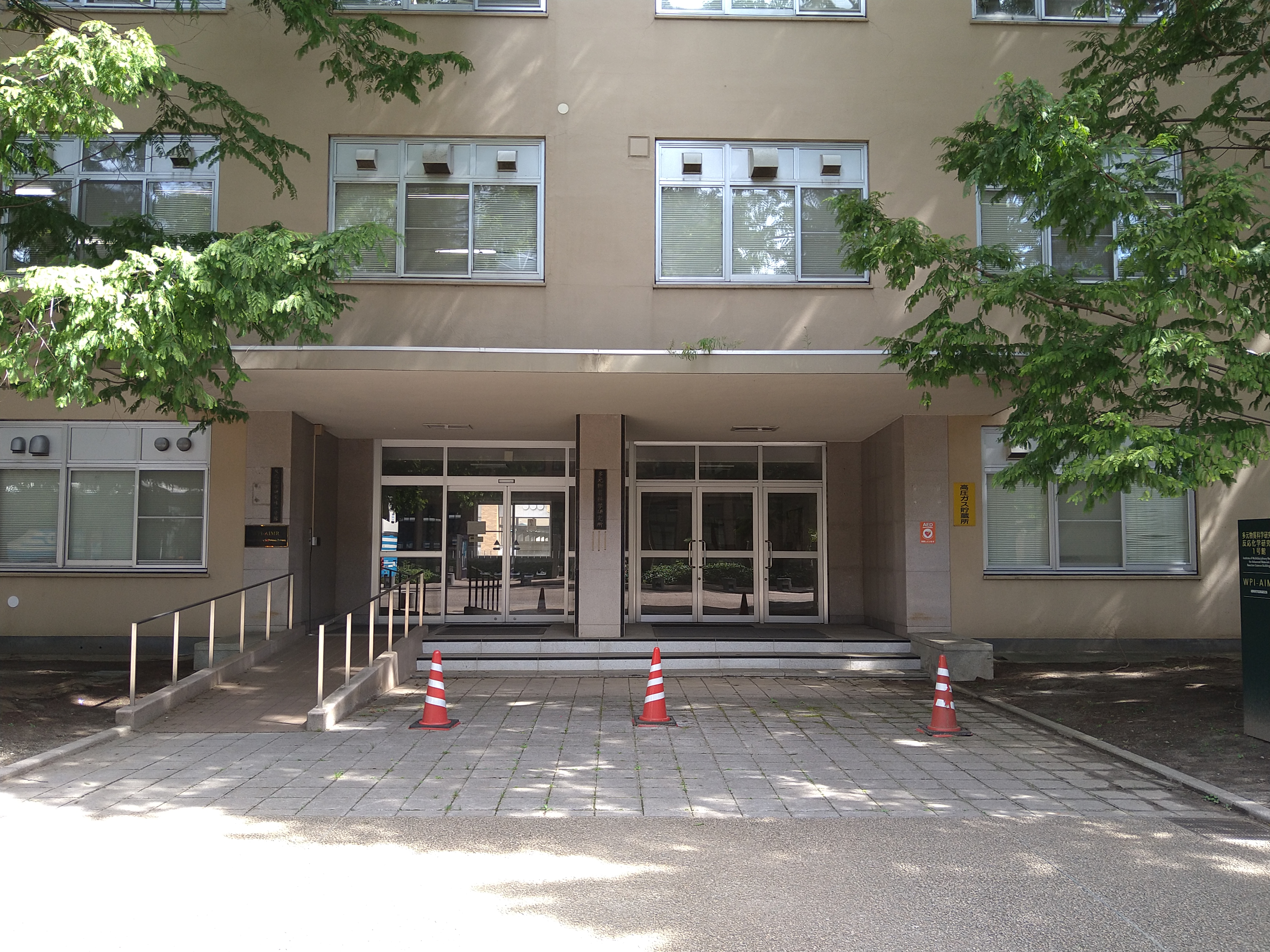
アクセス Accsess
| 連絡先 Contact | |
| 〒980-8577 宮城県仙台市青葉区片平2-1-1 2-1-1 Katahira Aobaku Sendai Miyagi 980-8577 | |
| 東北大学片平キャンパス 材料科学高等研究所 AIMR別館 317号室 317 AIMR Annext Katahira Campus Tohoku University | |
| Tel 022-217-5949 Tel +81-(0)22-217-5949 | |
|
准教授 森下 弘樹 hiroki.morishita.d8tohoku.ac.jp Associate Professor Hiroki Morishita hiroki.morishita.d8tohoku.ac.jp |
News
2026
2026/05/22 中村特任研究員が第60回(2026年春季)応用物理学会講演奨励賞を受賞しました。おめでとうございます!
講演タイトル:走査型光電流顕微鏡による単一NV中心画像の空間分解能
2026/04/23 川崎君(B4)が加入しました。
2026/04/01 中村特任研究員が着任しました。
2026/03/31 石橋博士が大阪大学基礎工学研究科に助教として栄転されました。
2026/03/23 中村君が博士を取得されました。おめでとうございます!
2026/02/27 中村君(D3)がX-nics学生発表会にて、プレゼンテーション賞を受賞しました。おめでとうございます!
2026/02/ 中村君(D3)が講演が、第73回 応用物理学会 春季学術講演会の注目講演に選ばれました。講演タイトル:走査型光電流顕微鏡による単一NV中心画像の空間分解能(講演番号:18p-W9_324-8)
2026/01/25 “コンパクトなポータブル量子センサの開発,”がニューダイヤモンド, vol.42, pp. 26-27 (2026).がPublishされました。
2026/05/22 Dr. Nakamura has received the 60th (Spring 2026) Young Scientist Presentation Award from JSAP. Congratulations!
Title of the presentation: Image Resolution of Single NV Center with Scanning Photocurrent Microscopy
2026/04/23 Mr. Mitsuki Kawasaki joined our lab as B4.
2026/04/01 Dr. Nakamura as Specially Appointed Research Fellow joined our lab.
2026/03/31 Dr. Ishibashi has been appointed as an Assistant Professor at the Graduate School of Engineering Science, Osaka University, marking a significant step forward in his career.
2026/03/23 Mr. Nakamura received his Ph.D. degree. Congratulations!
2026/02/27 Mr. Nakamura (D3) recieved the Best presentation award at X-nics Student Preseitaion.
2026/02/ Mr. Nakamura (D3) has been selected as a Highlighted Speaker at the 73rd JSAP Spring Meeting. Title of the presentation: Image Resolution of Single NV Center with Scanning Photocurrent Microscopy (Presentation No.: 18p-W9_324-8)
2026/01/25 “Compact and Portable Quantum Sensor Using Diamond NV Center,” New Diamond, vol.42, pp. 26-27 (2026). is published.
2025
2025/12/01 中村君(D3)の論文、“Scanning Photocurrent Imaging Resolution of Single NV Center in Diamond,” Applied Physics Letters 127, 224003 (2025).がPublishされました。 おめでとうございます!
2025/10/01 石橋一晃特任研究員、D1 Devsharma Sushen Chandraが加入しました。
2025/07/25 森下准教授が創発的研究支援事業「NV 量⼦スピントロニクスデバイスの創出」(代表:森下弘樹)に採択されました。
2025/07/08 “Compact and portable pulsed measurement module using diamond NV centers,” Japanese Journal of Applied Physics 64, 070903 (2025) がPublishされました。
2025/06/27 森下准教授が科研費挑戦的研究(萌芽)「単一核スピンの電気的電気共鳴検出技術の確立」 (代表:森下弘樹)に採択されました。
2025/06/11 森下准教授が村田学術振興・教育財団の2025年度研究助成に採択されました。
2025/12/03 Mr. Nakamura paper, “Scanning Photocurrent Imaging Resolution of Single NV Center in Diamond,” Applied Physics Letters 127, 224003 (2025) is published. Congratulations!
2025/10/01 Dr. Kazuaki Ishibashi as Specially Appointed Research Fellow and Mr. Devsharma Sushen Chandra as joined our lab.
2025/07/25 Assoc. Prof. Morishita accepted Fusion Oriented REsearch for disruptive Science and Technology (FOREST)
“ Development of NV Quantum Spintronics Device ” was adopted.
2025/07/08 “Compact and portable pulsed measurement module using diamond NV centers,” Japanese Journal of Applied Physics 64, 070903 (2025) is published.
2025/06/27 Assoc. Prof. Morishita accepted JSPS KAKENHI Grant-in-Aid for Challenging Research (Pioneering) “ Establishment of an electrical detection technique of single nuclear spin electronic resonance. ”.
2025/06/11 Assoc. Prof. Morishita accepted Murata Science and Education Foundation.
2024
2024/04/08 森下准教授が旭硝子財団の2024年度研究助成に採択されました。
2024/04/04 B4 川島君が加入しました。
2024/02/28 森下准教授がIOP Outstanding Reviewer Awards 2023, Applied Physics Expressを受賞しました。
2024/04/08 Assoc. Prof. Morishita accepted Asahi Galass Foundation.
2024/04/04 Mr. Morio Kawashima joined our lab as B4.
2024/02/28 Assoc. Prof. Morishita recievd IOP Outstanding Reviewer Awards 2023, Applied Physics Express.
2023
2023/10/25 Luding Wang助教が加入しました。
2023/09/25 内閣府・戦略的イノベーション創造プログラム(SIP) 「固体量子センサの社会実装促進に向けた実践環境の構築」(代表:大島武)が採択されました。
2023/08/01 “ ダイヤモンド中のNV-センタの電気的励起発光, ” ニューダイヤモンド, vol.39, pp. 19-23 (2023).がPublishされました。
2023/07/01 “ ダイヤモンド NV 中心の電子・核スピンの電気的検出, ” 応用物理, vol.92, pp. 425-429 (2023).がPublishされました。
2023/06/07 “Compact and portable diamond NV sensor module,” Applied Physics Express 16, 062004 (2023) がPublishされました。
2023/05/01 B4の三沢君が加入しました。
2023/04/01 中村君が加入しました。
2023/03/20 “Spin-dependent dynamics of photocarrier generation in electrically detected nitrogen-vacancy-based quantum sensing,” Physical Review Applied 19, 034061 (2023) がPublishされました。
2023/03/09 IOP Outstanding Reviewer Awards 2022, Japanese Journal of Applied Physicsを受賞しました。
2023/02/14 “Electroluminescence of negatively charged single NV centers in diamond,”Applied Physics Letters 122, 072101 (2023) がPublishされました。
2023/01/12 研究室HPの立ち上げ
2023/01/01 森下研究室が発足
2023/09/25 Cross-minister Strategic Innovation Promotion Program (SIP) “ Constraction of a Prtactical Enviroment of Solid Qunantum Sensors for Social Implementation. ” was adopted.
2023/07/01 “ 2023/08/01 “ Electroluminescence of Negatively Charged Single NV Centers in Diamond , ”
New Diamond, vol.39, pp. 19-23 (2023). is published.
2023/07/01 “ Electrical detection of electron and nuclear spins of NV centers in diamond, ”
Oyo Buturi, vol.92, pp. 425-429 (2023). is published.
2023/06/07 “Compact and portable diamond NV sensor module,” Applied Physics Express 16, 062004 (2023) is published.
2023/05/01 Mr. Tatsuki Misawa joined our lab as B4.
2023/04/01 Mr. Nakamura joined our lab as D1.
2023/03/20 “Spin-dependent dynamics of photocarrier generation in electrically detected nitrogen-vacancy-based quantum sensing,” Physical Review Applied 19, 034061 (2023) is published.
2023/03/09 IOP Outstanding Reviewer Awards 2022, Japanese Journal of Applied Physics is received.
2023/02/14 “Electroluminescence of negatively charged single NV centers in diamond,”Applied Physics Letters 122, 072101 (2023) is published.
2023/01/12 Launch of our webpage.
2023/01/01 Morishita Laboratory was established.
リンク
Link
東北大学
https://www.tohoku.ac.jp/
東北大学先端スピントロニクス研究開発センター(世界トップレベル研究拠点)(CSIS)
https://www.csis-crc.tohoku.ac.jp/
東北大学 スピントロニクス学術連携研究教育センター(CSRN)
https://www.csrn.tohoku.ac.jp/
東北大学 材料科学高等研究所(AIMR)
https://www.wpi-aimr.tohoku.ac.jp/jp/
東北大学 材料科学高等研究所(AIMR)水上研究室
https://www.wpi-aimr.tohoku.ac.jp/mizukami_lab/
Tohoku University
https://www.tohoku.ac.jp/en/
Center for Science and Innovation in Spintronics, Tohoku University (CSIS)
https://www.csis-crc.tohoku.ac.jp/en/
Center for Spintronics Research Network, Tohoku University (CSRN)
https://www.csrn.tohoku.ac.jp/en/
WPI Advanced Institute for Materials Research, Tohoku University (AIMR)
https://www.wpi-aimr.tohoku.ac.jp/en/
Mizukami Laboratory, WPI Advanced Institute for Materials Research, Tohoku University (AIMR)
https://www.wpi-aimr.tohoku.ac.jp/mizukami_lab/en/